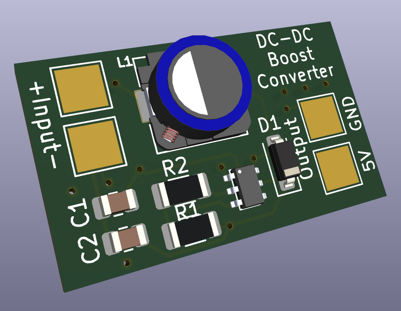
A DC-DC boost converter is a type of power converter that steps up (boosts) a DC voltage to a higher level. It is useful in applications where a higher voltage level is required than what is available from the input source. The boost converter typically consists of an inductor, a switch (usually a transistor), a diode, and a capacitor.
Power supply requirements:
- Input Voltage 1.0 ~ 3.5 V
- Output Voltage 5.0 V
- Output Current 100 mA
The topology of DC-DC boost converter is different from buck converters, and usually they are used with battery powered devices. Voltage boost is require if battery voltage supply is not sufficient to power up the majority ICs.
I choose to base my power supply design around Analog Devices LTC3429.
The LTC3429 component is a high efficiency 500 kHz adjustable output voltage boost converter, and it meets the requirements as this regulator’s get 0.5V to 4.4V input voltage and adjustable output voltage from 2.5V to 4.3V and the output voltage can be increased up to 5V if an additional Schottky diode is included.
This regulator comes with useful additional functions, such as:
- Low Voltage Start-Up – this regulator can activate even when the supply voltage is as low as 0.85V. However, if the supply battery drops below 0.85V due to discharge, there is a possibility that the regulator may not start.
- Soft-Start – this feature ensures that the regulator delays activating the output voltage by 2.5 ms after the power source (battery) is connected to the device. This soft-start function enables the regulator’s oscillator to stabilize at the correct frequency before beginning operation as a switching power supply.
- Anti-ringing control – is a feature that prevents high-frequency ringing on the SW pin, reducing the electromagnetic interference (EMI) generated by the regulator.
- Short circuit protection – this feature enables the circuit to be shorted without harming the regulator. It rapidly discharges the internal capacitor, effectively shutting down the IC and protecting both the regulator and the circuit.
Simplified Schematic from datasheet

The first step, the output voltage feedback resistors were determined using the formula below, as specified in the datasheet:

High resistor values were selected to maintain high efficiency under light load conditions.
R2 was selected as 255 kΩ, and the value of the R1 resistor was then determined using the following formula:

because this is not a standard value, I choose 768k Ohm for R1 resistor.
this provides output of :
![]()
Lehosif tmona shel divider from scheme
Capacitor selection (from datasheet, page 9)

Considering that the input capacitor’s DC voltage rating can be as low as 4 V or 6.3 V due to the relatively low input voltages, it is advisable to use an output capacitor with a DC voltage rating of at least double the recommended value. Ceramic capacitors are known to exhibit a DC bias effect, which can substantially reduce their capacitance at specific voltages.
Inductor selection:
The LTC3429/LTC3429B can utilize small surface mount and chip inductors due to its fast 500kHz switching frequency. Typically, a 4.7µH inductor is recommended for most applications. Larger values of inductance will allow greater output current capability by reducing the inductor ripple current. Increasing the inductance above 10µH will increase size while providing little improvement in output current capability. The approximate output current capability of the LTC3429 versus inductance value is given in the equation below and illustrated graphically in Figure below:

A high inductance value of 22uH was selected for the inductor to ensure the regulator maintains efficiency at the desired output current.
Diode selection:

The shutdown pin (SHDN), when inverted, should be connected to VIN to ensure the regulator operates without the need for an external controller or supervisor IC. This configuration enables the regulator to function whenever a power source within the acceptable input voltage range is connected.
The goal is to achieve the shortest possible current loop. The following recommended design provided by the datasheet


