A DC-DC buck regulator is a type of voltage regulator that steps down a higher voltage to a lower voltage.
The buck regulator operates by controlling the duty cycle of a switching transistor to regulate the output voltage.
It is called a “buck” regulator because the output voltage is lower than the input voltage, and the switching action helps reduce or “buck” the voltage.
The goal is to design a DC-DC buck converter PCB layout.
Switching power supplies are very common as they offer high efficiency, and therefore do not typically require thermal management as a linear supply would.
Power supply requirements:
- Input Voltage 7.0 ~ 14.0V
- Output voltage 5.0V
- Output Current 1.0A
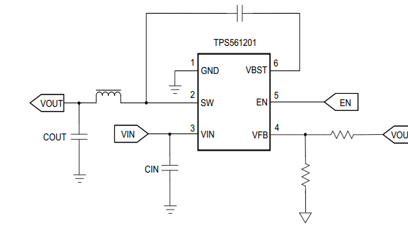
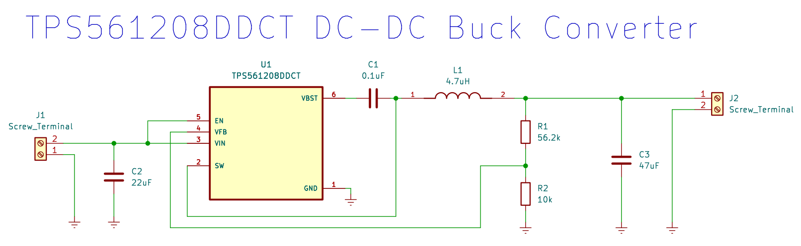
I choose to base my power supply design around Texas Instruments TPS561208DDCR, because it meets the requirements as it has a 4.5V to 17V input voltage and adjustable output voltage from 0.76V to 7V.
Simplified Schematic from datasheet
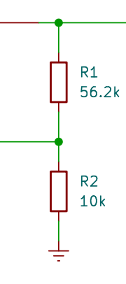
From the Datasheet , I choose the output voltage resistors to set the output voltage to 5V.
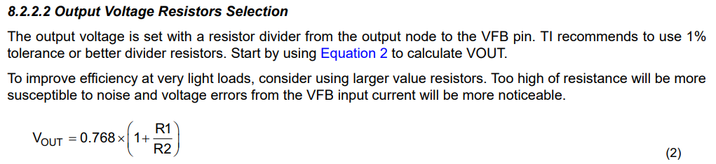
If I choose low values of resistors, it would mean that the converter is less susceptible to noise, and at the same time the efficiency with light loads would decrease.
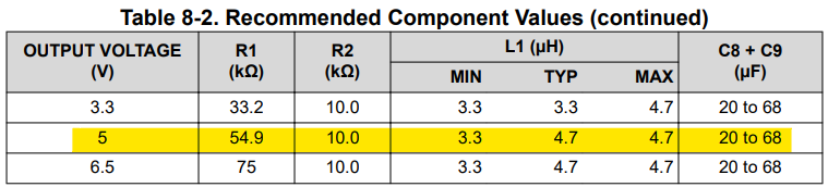
The value of resistor R2 was selected as 10k Ohm from the recommended table in the datasheet,
and then the R1 value was calculated from the formula
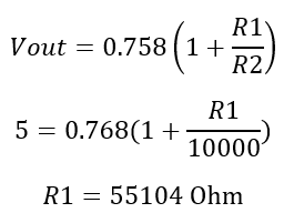
55.104k Ohm is not a standard value of resistor, I choose 56.2k Ohm value wich provides output of 5.08V
![]()
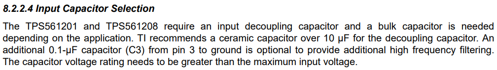
The datasheet recommends an input capacitor of 10uF or larger. Capacitance of 22uF was chosen.
The value for the inductor was chosen from the recommended component values table – 4.7uH.
To insure stable inductance value and ensure our inductor will not get too hot we need to choose inductor which is rated for more than 1A of saturation current and rated current.
As the load on the circuit is not necessarily the load on the inductor and this can be a critical factor when selecting the right component.
I’m using the recommended output capacitor value from the table in the datasheet.
The output capacitance is recommended from 20 to 68uF for a stable converter, so I choose middle value of 47uF capacitor.
We might choose to add significantly higher capacitance if we have a rapidly changing load on the supply.

In addition to the input and output capacitors, a bootstrap capacitor is required for proper operation.
The manufacturer recommends a value of 0.1uF ceramic capacitor.
Schematic
Before jump into the routing process, we can find in the datasheet recommended layout guidelines, layout example and design tips from the datasheet
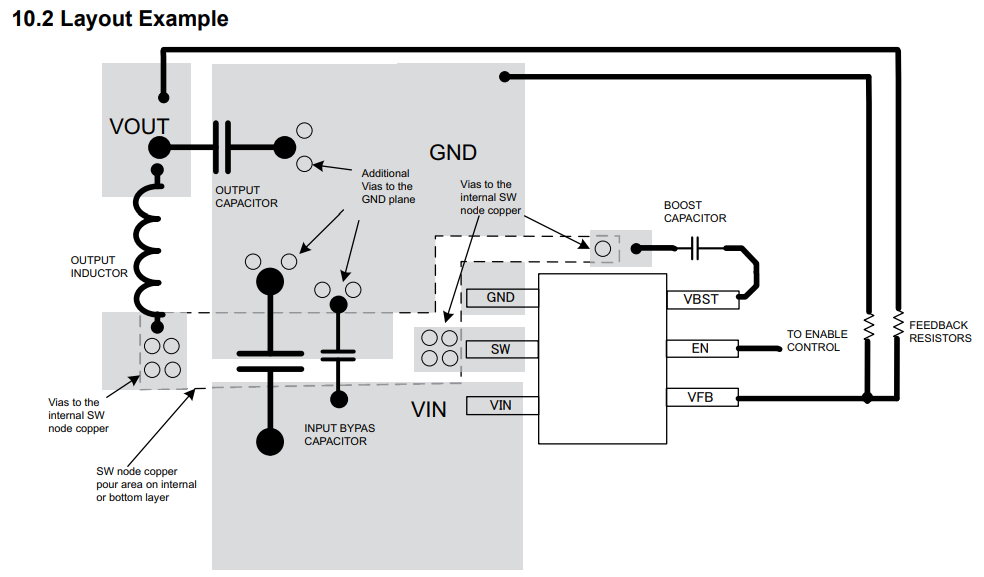
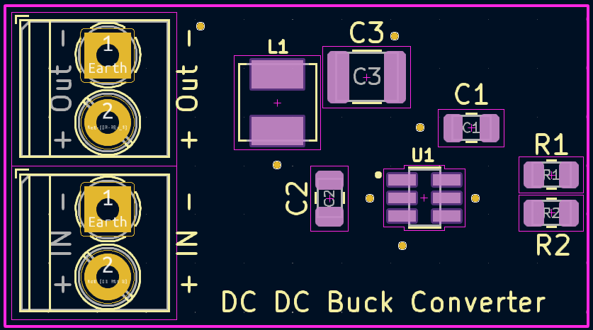
The first step of the layout is to locate components in the right place, like in the layout example but with slight modifications to accommodate the components chosen.
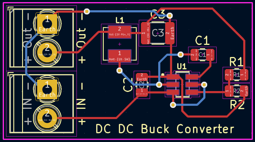
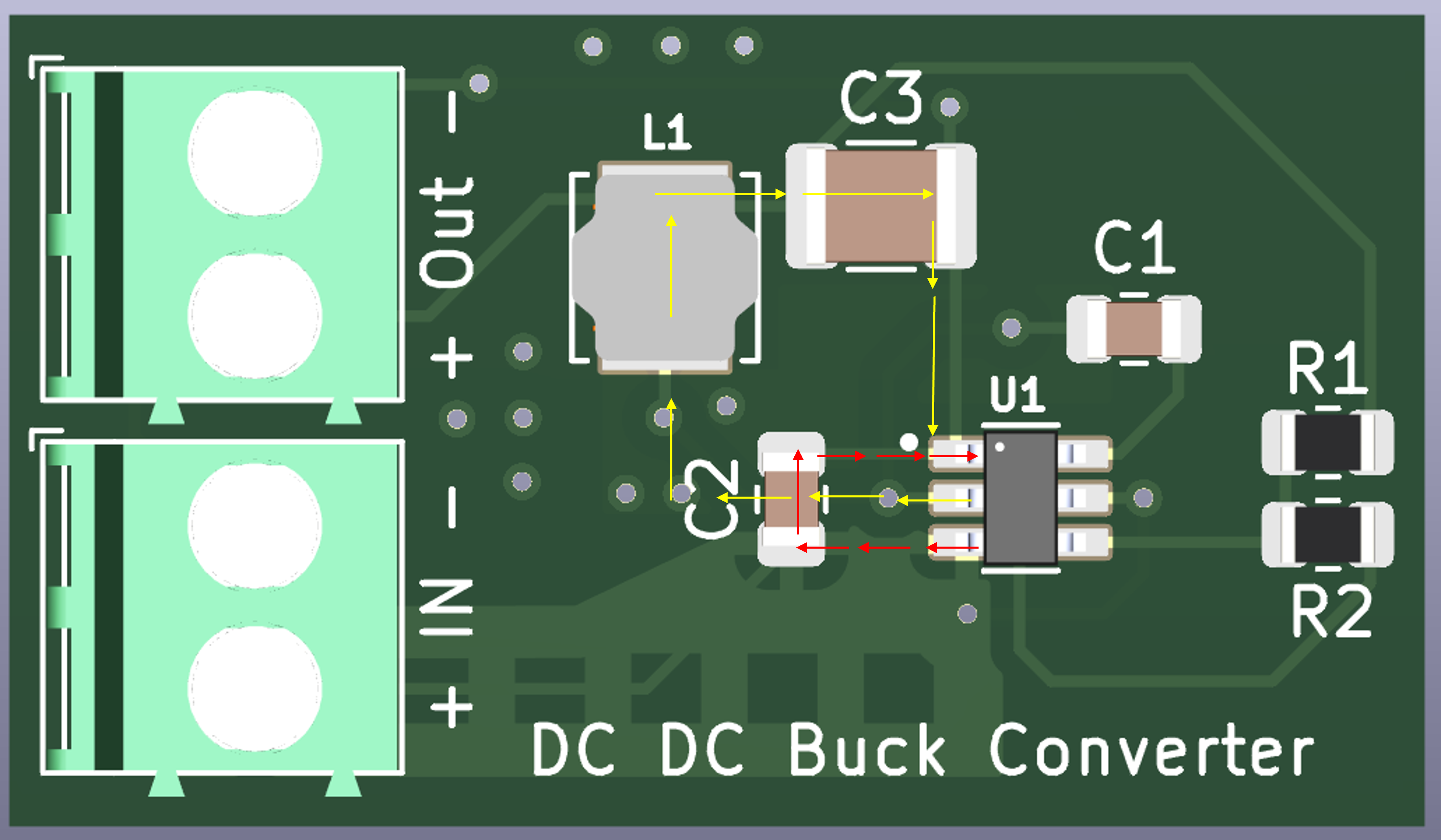
The second step was to manually route all the traces. This step is needed to follow the current flow through the input and output loops and through the circuit.
The third step is to add polygons to the input and output loops so that we would achieve as low an impedance as possible
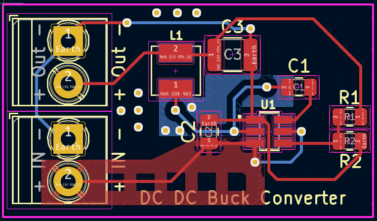
The current loops of the layout
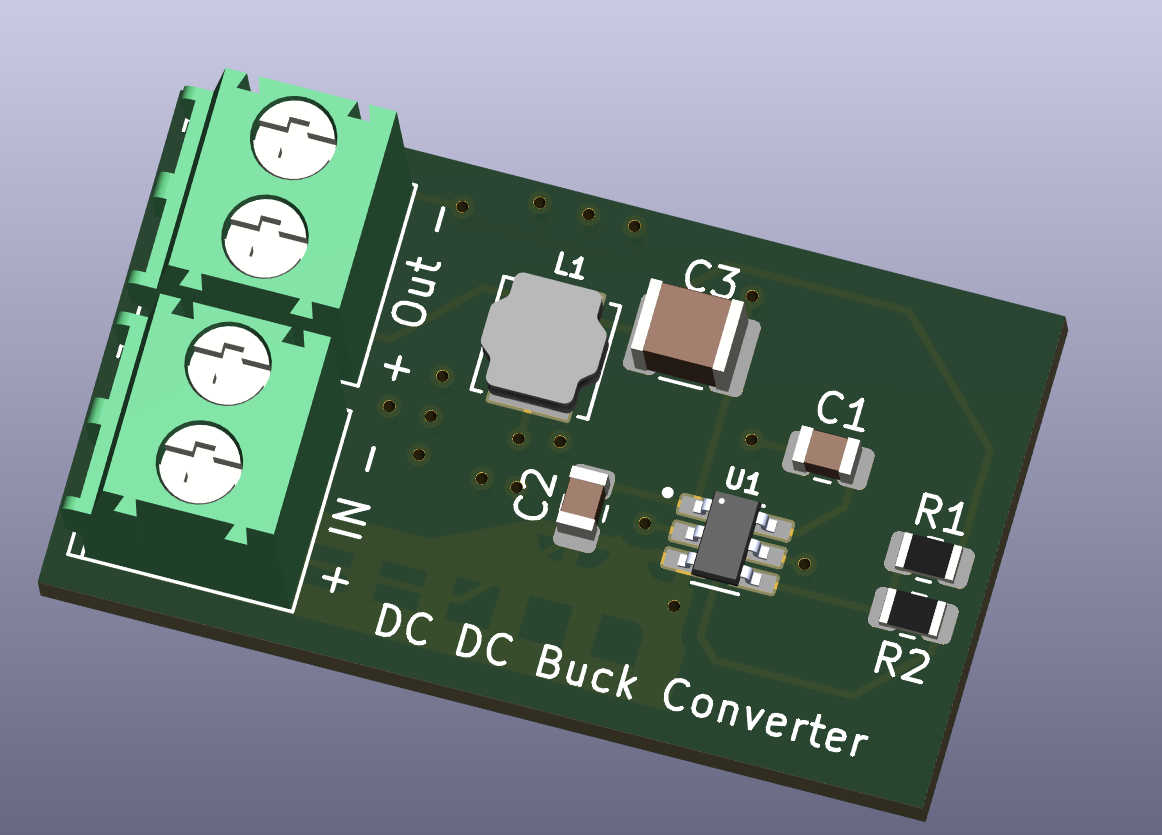
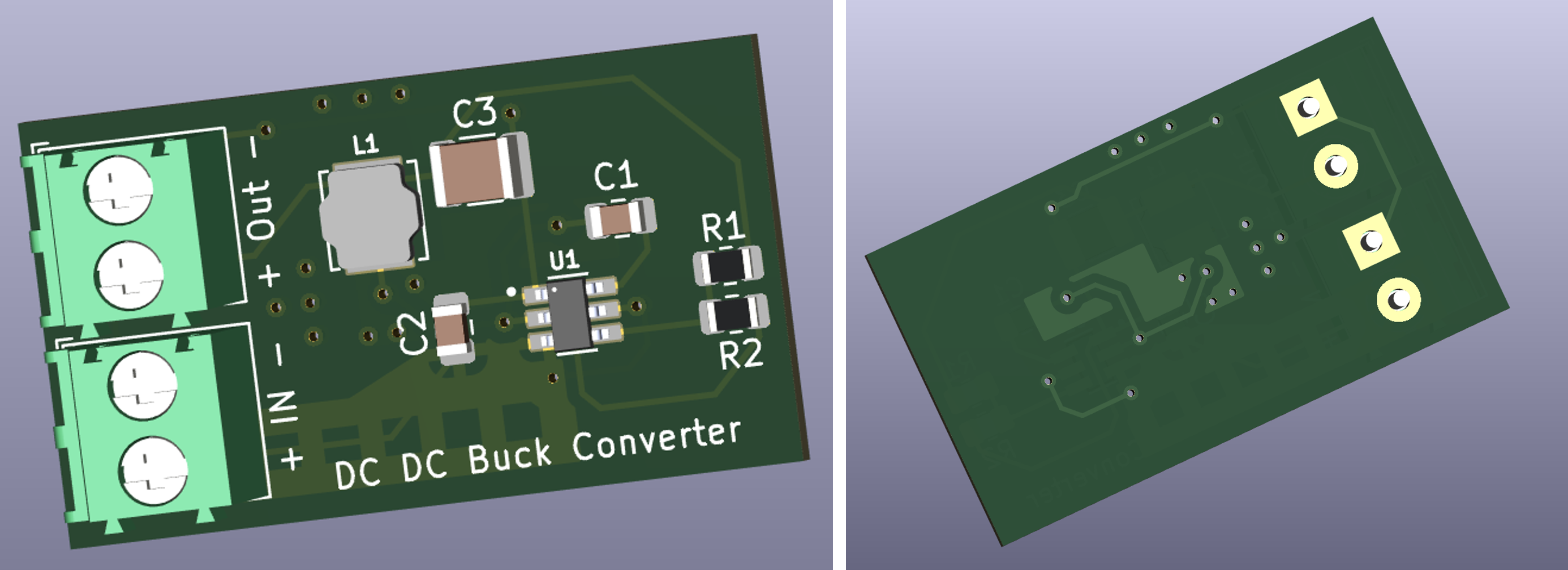
3D Model
Conclusion
- Designing a simple DC-DC buck layout requires careful consideration to avoid additional noise, excess electromagnetic radiation, and instability.
- When designing adjustable output voltage regulators, the output voltage divider must be chosen wisely to balance efficiency and noise susceptibility.
- Input capacitor selection is complex and must consider input voltage ripple, noise, and current demands to avoid EMC certification challenges.
- Inductor selection for switched-mode voltage regulators is critical to ensure efficient operation and avoid saturation.
- Output capacitor type and parameters significantly impact conducted noise on the output voltage rail.
- PCB layout is critical, with short and wide traces for current loops, easy paths for capacitor pins, and short, circular current loops to reduce EMI.